Thursday 11 June 2015

Week 18 (FYP II): Submission of FYP Report

This the last post of this blog. 

Tomorrow, 12th June 2015, I will submit the following:

  1. The softcopy and hardcopy files related to the "Thermoelectric Devices Charger" to the Supervisor.
  2. The softcopy files related to the "Thermoelectric Devices Charger" to the FYP online website.
  3. A hard cover of the final year project report to the library.
If all goes well, the FYP subject will be completed. 

Mohamad Shafiq Bin Hairudin
51210111372
Student of UNIKL BMI
BET in Electrical.

Saturday 6 June 2015

Week 15,16,17 : Full Report Writing and Final Exam S1'2015

Objective:
To complete and finalize on full report writing.

Analysis/Discussion:
Due to final exam S1'2015 my progress on report writing has little progress because of my other subject that was included in final exam. I had to study and at the same time finishing my full report writing, video and others as the following format that state in website FYP UniKL BMI.

Conclusion:
I must managed to complete the project full report within the time given

Reference:
  1. http://fyp.bmi.unikl.edu.my/index.php

Thursday 14 May 2015

Week 14 : Poster Designing and Project Demo Presentation

Objective: 
Designing poster for project demo presentation and demonstration the project.
 
Analysis/Discussion:
The presentation day of FYP II is on 13th May 2015 at Gemilang Hall. All candidates that participate need to prepare for presentation according the format given. As it has been briefed before the format of poster for presentation must contain the following subject:  
  1. Introduction
  2. Objectives
  3. Methodology
  4. Block Diagram
  5. Analysis
  6. Conclusion

My poster was design following the format:

Figure 19: Poster for project demo presentation

Conclusion:
The Presentation Day has been a success. I have presented my project to both of the assigned accessors and they are satisfied with my project.

Thursday 7 May 2015

Week 13 : Testing and Troubleshooting

Objective:
Testing of functional "Thermoelectric Devices Charger" and troubleshooting when problem occur.

Analysis/Discussion:
As the prototype have been completely constructed, there is need to testing and verify that the system is surely able to supply low powered devices through "Thermoelectric Devices Charger" .For testing purpose, the smartphone and power bank was used. it is successfully work for charging purpose as shown in figure below.
Figure 14: Ice used for the best output of "Thermoelectric Devices Charger"

Figure 15: Heat source from the candle to hot side of "Thermoelectric Devices Charger"

Figure 16: Measuring output thermoelectric and output "Thermoelectric Devices Charger"

 Figure 17: Result of "Thermoelectric Devices Charger"

Due to testing and troubleshooting of prototype, all data has been recorded in a graph. In graph shown below is the graph when ice used to steel container (cold side of thermoelectric) and candle (as heat source as hot side).
 Figure 18: Recorded result of "Thermoelectric Devices Charger"

Conclusion:
The prototype is successfully function based on objective requirement development of "Thermoelectric Devices Charger"

Friday 1 May 2015

Week 12 : Designing the Thermoelectric Device Charger

Objective:
To design which compatible to bring anywhere.

Analysis/Discussion:
This design based on the best output can be produced by the thermoelectric. I have selected TEC1-12708 and DC-DC booster converter to develop "Thermoelectric Device Charger".

Figure 13: Design of "Thermoelectric Device Charger"

Conclusion:
The steel container is to fill the water or to fill the ice for cold side of thermoelectric and at hot side of thermoelectric are used heat from candle or campfire.

Wednesday 22 April 2015

Week 11 : FYP Briefing 3

Objective:
To attend FYP Briefing 3 at TTL 1.

Analysis/Discussion:
Today, I attend third fyp briefing at TTL hall handle by fyp committee. The FYP committee explained briefly about:
  1.  Project Demo Preparation
  2.  Final report compilation
Discussion:
I had doing my project's report followed as the format given and preparing for the project demo presentation.

Saturday 18 April 2015

Week 9,10 : Joule Thief Circuit

Objective:
To design, develop and testing of joule thief circuit

Analysis/Discussion:
A "Joule Thief" is a simple voltage booster circuit. It can increase the voltage of power source by changing the constant low voltage signal into a series of rapid pulses at a higher voltage. You most commonly see this kind of circuit used to power LEDs with a "dead" battery. But there are many more potential applications for this kind of circuit. 

In this project, I am going to show you how you can use a Joule Thief to charge batteries with low voltage power sources. Because the Joule Thief is able to boost the voltage of a signal, you are able to charge a battery with a power source whose output voltage is actually lower than the battery itself.
This lets you take advantage of low voltage power sources such as thermoelectric generators, small turbines and individual solar cells. 

Picture of Modified Joule Thief That Can Act as a Battery Charger
 Figure 10: Circuit diagram for joule thief charging circuit

Here are the materials and tools that you will need to complete this project.

  • Ferrite toroid core
  • Insulated Wire
  • NPN Transistor (2N2222, 2N3904, or similar)
  • 0.01 microfarad Capacitor (capacitor code:103)
  • 330 microfarad Capacitor
  • 1 kohm resistor
  • 6V Zener Diode
  • Diode
 
In order to make a battery charger, I made a few changes to the standard Joule Thief Design. 

First I added a capacitor to the node between the resistor and the first coil. This helps to stabilize the output a little. 

Then I added a zener diode to the base of the transistor. This helps to protect the transistor from being damaged by voltage spikes. The Emitter-Base junction is the weakest point of the transistor. Most small NPN transistors will have a maximum allowable Emitter-Base voltage of 6 volts or less. So I added a zener diode between the base and the collector of the transistor. The diode prevents the Emitter base junction from becoming reversed biased.

At the output of the second coil, I added a diode. This allows the output voltage to pass through but it prevents electricity from the battery draining back through the transistor. 

The capacitors and the zener diode also help protect the transistor from high voltage spikes that can occur if the circuit is turned on without a load. The voltage of the second coil will jump up as much as it needs to in order to be discharged. If there is no load attached, the coil voltage can reach over 60 volts. This could quickly damage the transistor. The zener diode and the capacitors help to limit these voltage spike.

Picture of Prototype the the Circuit on a Breadboard 
Figure 11: Pretesting the circuit

Picture of Solder the Circuit Together on a Circuit Board 
Figure 12:  Finalize the circuit

Conclusion:
The input voltage will affect how high the output voltage can get. With the components that I used you will get the best performance from power sources that are between 0.9 volts and 2.0 volts (with a maximum at 1.50 volts). Below 0.9 volts, the circuit will have difficulty boosting the voltage to a high enough to effectively charge a battery. Above 2.0 volts the output voltage will can start to get to high and it will be limited by the zener diode that is protecting the transistor.

Reference:
  1. http://www.electronics-lab.com/blog/?tag=joule-thief
  2. http://www.evilmadscientist.com/2007/weekend-projects-with-bre-pettis-make-a-joule-thief/
  3. https://lockerdome.com/6391315667620929/7385521946113556

Saturday 4 April 2015

Week 6,7,8: DC-DC Booster Converter

Objective:
To design, develop and testing of selected DC-DC booster circuit.

Analysis/Discussion : A voltage step-up is a circuit that increases the voltage. It can be AC/AC, AC/DC, DC/AC or DC/DC. This voltage step-up is a DC/DC adjustable voltage regulator. Usually a voltage regulator is fed by a higher input than output voltage, for example 9V IN to 5V OUT. This circuit will take a low voltage (down to 0.7V) and step it up to adjustable 2.7-5.5V. Since it is a regulator, the output voltage will stay constant regardless input voltage (0.7-5.5V), as long as output voltage is higher than input. It cannot step-down, only step-up. Are there any ICs that can do both?

This is a typical circuit for a battery-powered USB-charger, for example single  AA batteries (1.5V) to power 5V USB. There are tons of DIYs how to create that. They are often hard-specified to 5V output power. This construction can be used in a range of other applications. Many electronic devices work within 3-5 V and often you want to power them by low voltage power sources.


Picture of Materials 
 Figure 7: Circuit diagram for DC-DC booster converter

List of component used in the circuit:
  • IC (DC-DC step-up): MAX757CPA+ - IC, DC/DC UP CONVERTER, DIP8, 757
  • Socket (DIP8): TE CONNECTIVITY / AMP - 1-390261-2 - SOCKET IC, DIL, 0.3", 8WAY 
  • C1 (150µF): PANASONIC - EEUFR1H151, RADIAL, 50V, 150UF 
  • C2 (100µF): PANASONIC - EEUFC1H101, RADIAL, 50V, 100UF 
  • C3 (0.1µF): EPCOS - B32529C104J, FILM, 0.1UF, 63V, RADIAL
  • C4 (1µF): EPCOS - B32529C105J, FILM, 1UF, 63V, BOXED 
  • D1 (1N5817): VISHAY FORMERLY I.R. - VS-1N5817, SCHOTTKY, 1A, 20V 
  • D2 (LED): MULTICOMP - 703-0100, 5MM, RED, 400MCD, 643NM
  • L1 (22µH): PANASONIC - ELC16B220L, 22UH, 4.6A, 0R031
  • P1R1 (10kΩ): MULTICOMP - MF25 10K, 10K, 0.25W, 1%
  • R1&P1R2 (47kΩ): MULTICOMP - MF25 47K, 47K, 0.25W, 1% 
  • R2 (470Ω): MULTICOMP - MF25 470R, 470R, 0.25W, 1%
  • P1(100kΩ): TE CONNECTIVITY / CITEC - CB10LH104M, SIDE, 100K 
These item is easily to get in electronic store in Kuala Lumpur. At down below is the specification of Max757 IC.

  • Minimum start-up voltage (@10mA load): 1.1V
  • Minimum start-up voltage (@300mA load): 1.7V
  • Minimum operating voltage (@20mA load): 0.7V
  • Input voltage range: -0.3 to +7V
  • Output voltage range: 2.7 to 5.5V
  • Maximum output load (@input voltage=2V): 200mA@5V, 300mA@3.3V
  • Maximum output load (@input voltage=1V): 50mA@5V, 75mA@3.3V
  • Efficiency: Max 87% (depends on input voltage and output load
  • Quiscent current (@no load, 2V input, 3.3V output): 60µA
  • Operating temperature: 0ºC to +70ºC (Using Max75_C__) 
 Full specification for max757 can be found in this pdf:
http://pdfserv.maximintegrated.com/en/ds/1167.pdf 


Picture of Pre-Test 
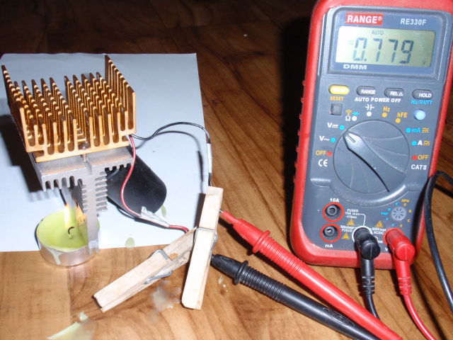
Figure 8: Pretesting the circuit

I measured the output voltage to be as adjustable as before (2.77-5.39V). I measured efficiency at 2.5V/340mA in and 4.94V/150mA out. Converted to watts, (4.94*0.150)/(2.5*0.340)=0.74/0.85W, gives 87% efficiency. That is exactly according to spec but I got less efficiency at lower output load, but still expected. For full efficiency you need better components and a more compact layout. Some connections should not be more than 5mm according to PDF. There are two free copper lanes in my layout that can be utilized as common ground, I tried that too but got exactly the same result. It can also be my 10 year old multi-meter that is not calibrated.

I also measured the efficiency at maximum power. I had 3V/900mA in and 4.66V/460mA out. Converted to watts, (4.66*0.46)/(3*0.9)=2.14/2.7W, gives 79% efficiency. 

I also successfully charged an iPhone 4s with it. It charge at 500mA with 3V in and 4.7V out. Decreasing the input voltage to 2V gives 4.4V out at 300mA (which is quite slow charging). The maximum charge for iPhone is 5V/1A from standard charger.


Result from testing in various input:
2V in => 4.4V*300mA=1.3W out
3V in => 4.7V*500mA=2.35W out
4V in => 4.95V*500mA=2.5W out

Picture of Testing and Finishing 
Figure 9: Finalize the design of DC-DC booster converter

Conclusion:
This circuit can be determined to use in thermoelectric device charger but the output current is too small to charge the devices. It will gives longer duration of charging.

Reference:
  1. http://www.instructables.com/id/Battery-Charger-Powered-by-Fire/

Monday 2 March 2015

Week 5 : Testing on Seebeck thermoelectric module

Objective:
Testing the output Seebeck module of thermoelectric in various temperature

Analysis/Discussion:
After a couple of week, my order for tegtec.com has delivered. I made a testing on Seebeck module to verify the output in various temperature.
 
 
 Figure 5: Receipt from tegtec.com

 
Figure 6: Testing the output of Seebeck thermoelectric module

Below is result due to testing of the Seebeck thermoelectric module:
 
 
Table 2: Result from testing output Seebeck module in various temperature

Conclusion:
Seebeck module required high temperature to generate more voltage